How P and N Type Semiconductors Are Formed
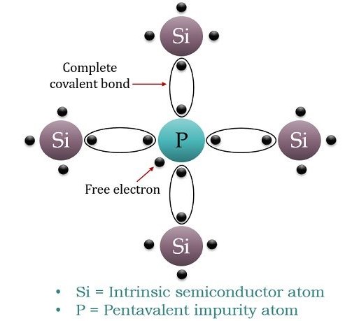
Contact or junction is the creating of a region between the p and n layers where p-type holes can recombine with n-type free electrons producing light such as in light emitting diodes LEDs. To explain the formation of N - type semiconductor let us introduce a pentavalent impurity atom into the lattice of.

N Type Semiconductor What Is It Diagram Explanation Electrical4u
P-n junctions form the basis of how a lot of current technology works by creating diodes.

. Semiconductors are two types. 12 rows P-type Semiconductor. P-type semiconductor is formed by adding trivalent impurities and N-type semiconductor is formed by adding pentavalent impurities in the semiconductor.
As components like gallium boron indium etc are doped to form a p-type semiconductor. Uses of p-type semiconductors. As opposed to n-type semiconductors p-type semiconductors have a larger hole concentration than electron concentration.
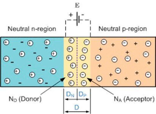
A P-N junction is an interface or a boundary between two semiconductor material types namely the p-type and the n-type inside a semiconductor. Here the type of semiconductor can be determined by the kind of impurity there. We can also refer to this as a difference between electron donors and acceptors.
As opposite an n-type semiconductor is created when group V elements are doped to an intrinsic semiconductor. The procedure of adding impurities to semiconductor materials is known as. Trivalent impurities like Aluminium Indium and Gallium are added to the intrinsic semiconductor.
The majority carriers in a p-type semiconductor are holes. Of free electrons in the host crystal. A crystal that has its conduction value in between conductor and insulator is termed as the semiconductorIt can be formed by the addition of impurities.
The P-type semiconductor can be formed by. A P - type semiconductor is formed when a small amount of trivalent impurity is added to pure Germenium or silicon atom crystal. The addition of trivalent impurity produces a large no.
The term p-type refers to the positive charge of the hole. The resulting p-n junction forms a depletion region under the Schottky junction that reduces leakage current through the Schottky diodes in. The extrinsic p-Type Semiconductor is formed when a trivalent impurity is added to a pure semiconductor in a small amount and as a result a large number of holes are created in it.
Charge Carriers are electrons in n type semiconductor the conductivity will increases due to the presence of these extra negatively charged electrons that why this type of semiconductor is not as the n-type semiconductor in our next is P type semiconductor in p type semiconductor at trivalent impurity that the group 13 elements is topped with the Silicon and Germanium that is a. An integrated circuit includes a Schottky diode having a cathode defined by an n-type semiconductor region an anode defined by a cobalt silicide region and a p-type region laterally annularly encircling the cobalt silicide region. An N - type semiconductor is formed when a small amount of pentavalent impurity is added to a pure Germenium or Silicon crystal.
P-type semiconductors are created by doping an intrinsic semiconductor with an electron acceptor element during manufacture. These materials are semiconductors like Si silicon or Ge germanium including atomic impurities. The addition of pentavalent impurity produces a large no.
Examples of pentavalent impurities are. A large number of holes are provided in the semiconductor material by the addition of trivalent impurities like Gallium and Indium. The p type semiconductor is formed when the Trivalent impurity is added to the pure semiconductor.
3 and 5 respectively. Therefore it creates an additional hole thus. May 31 2019 By WatElectronics.
Hence option B and C are correct. To explain the formation of P - type semiconductor let us introduce a trivalent impurity into the lattice of a pure silicon crystal. P-n junctions are formed by joining n-type and p-type semiconductor materials as shown below.
The p-side or the positive side of the semiconductor has an excess of holes and the n. In a pure semiconductor crystal each atom produces four covalent bonds with four neighbor atoms in the crystal. The addition of trivalent impurities such as boron aluminum or gallium to an intrinsic semiconductor creates these positive electron holes in the structure.
The PN-junction diode is made up of two adjacent parts of two semiconductor materials like p-type and n-type. In a diode current can flow easily in one direction but not the. In an n-type semiconductor pentavalent impurity from the V group is added to the pure semiconductor.
Energy band diagram for p-type semiconductor s. However in a p-n junction when the electrons and holes move to the other side of the junction they leave behind exposed charges on dopant atom sites which are fixed in the crystal lattice and are unable to move. It can be referred to as either p-type or n-type.
5 and 3 respectively. The trivalent atom has 3. P-type and N-type extrinsic semiconductors are formed by adding impurities of valency 3 and 4 respectively.
In p-type semiconductors holes are the majority carriers and electrons are the minority carriers. Formation of p type semiconductor material. Of holes to the host crystals.
Solve any question of Semiconductor Electronics. N-type semiconductors are created by doping an intrinsic semiconductor with donor impurities. Are needed to be.
A p-type semiconductor is created when group III elements are doped to a complete semiconductor material. A common dopant for n-type silicon is phosphorus. For example a silicon crystal doped with boron group III creates a p-type semiconductor whereas a crystal doped with phosphorus group V results in an n-type semiconductor.
Hence its conduction is based on the types and the amount of impurity added. Now to produce a p-type semiconductor trivalent impure atoms like Boron B Aluminum Al etc. Materials Devices And Simple Circuits with-.
N-Type semiconductors are formed by doping pure elements element such as Silicon Si and Geranium Ge having 5 valence electrons with pentavalent impurity such as Antimony Sb Arsenic As or phosphorus P having four valence electrons. The term p-type refers to the positive charge of a hole. 5 and 4 respectively.
The trivalent impurities added provides extra holes known as the acceptor atom.
P N Junctions And Band Gaps Band Gap Physics Band
Understanding The Difference Between N And P Type Semiconductors
Differences Between P Type And N Type Semiconductor Linquip
No comments for "How P and N Type Semiconductors Are Formed"
Post a Comment